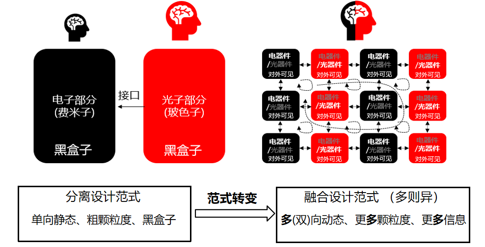
光电融合集成回路(芯片)定义:光电融合芯片是指通过一系列特定的加工工艺,将晶体管、光电二极管等电子和光子有源器件和电阻器、波导等电子和光子无源元件,按照一定的回路互连,“集成”在半导体(如硅或铟磷等化合物)晶片上,封装在一个外壳内,执行特定功能的回路或系统。关于光电融合芯片更加详细的概念和介绍,请参考本文献。
与集成电路、光子集成的关系: 集成电路侧重于电子之间的互相作用,光子集成侧重于光与物质的互相作用,光电融合芯片在集成电路和光子集成的基础上,进一步深入研究光子与电子通过物质互相作用的“集成”回路,加速光子和电子走向融合统一的进程。光电融合芯片把光子器件融入集成电路,通过借鉴集成电路的发展经验和方法论,丰富了集成电路的内涵并拓展了其边界,是后摩尔时代信息产业的重要发展方向。
Vision
Due to both physical and economic constraints, Moore's law is approaching to its end.
Meanwhile, new applications (e.g., IoT, artificial intelligence, big data, etc.) are emerging rapidly. The gap
between technology and demand continues to grow, creating a grand sustainability challenge for the
information industry. Combining photonics with electronics has been widely recognized as an effective
"More-than-Moore" solution to resolve this challenge. The convergence of photonics and electronics is now still in its single-transistor stage, and most research so far has been focused on device and integration technology. Over the last few years,
integrated photonic devices gradually grow mature. We are now ready to move into the circuit stage.
Nevertheless, the Electronic-Photonic Heterogeneously-converging Integrated Circuits
(EPHIC) faces many new challenges in terms of stability, energy efficiency, chip area, and so on. We aim to resolve
these challenges by leveraging our rich experiences in electronic integrated circuits and bring the convergence
of electronics and photonics to a new level.
For more details regarding our vision, please refer to this paper .